Bryan Tan (Chen Zhengyu) (CSD), Christy Lau Jin Yun (CSD), Xu Muzi (CSD), Kushagra Jain (EPD), Shamoeel Aliasgar Moochhala (EPD), Colin Teoh (EPD), Loo Jia Ying Sarah (EPD)
Instructors:
Edwin Koh
Writing Instructors:
Delfinn Tan Sweimay
Background
The Nanotechnology industry
uses special patterned moulds to produce extremely small, valuable devices and components. These devices are used in microchip, optics, and biotechnology applications.
Enlitho uses the powerful and precise Electron Beam Lithography (EBL) process to manufacture the aforementioned moulds. However, efficient mass manufacture of these moulds remains an industry challenge.
Applications
Microchips (GPUs and CPUs)
Optical Microlens (VR/AR Lens, Holograms)
Biotech Microfluidics (Lab-on-a-chip)
Industry Pain Points
Expensive
The immense cost of traditional nano-fabrication tools make them inaccessible to smaller labs and start-ups.
Slow
Traditional processes like Electron Beam Lithography (EBL) tend to be very slow, hindering mass production capabilities.
Manual
Manual imprinting and inspection are time-consuming and labour-intensive, as well as less effective at the nano-scale.
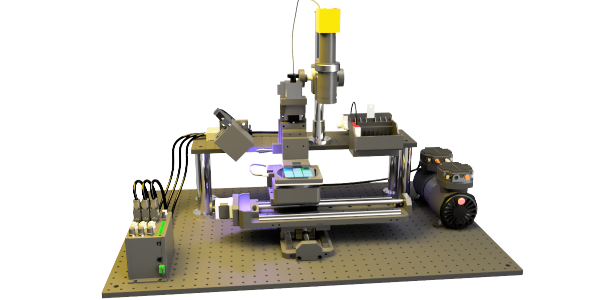
Solution:
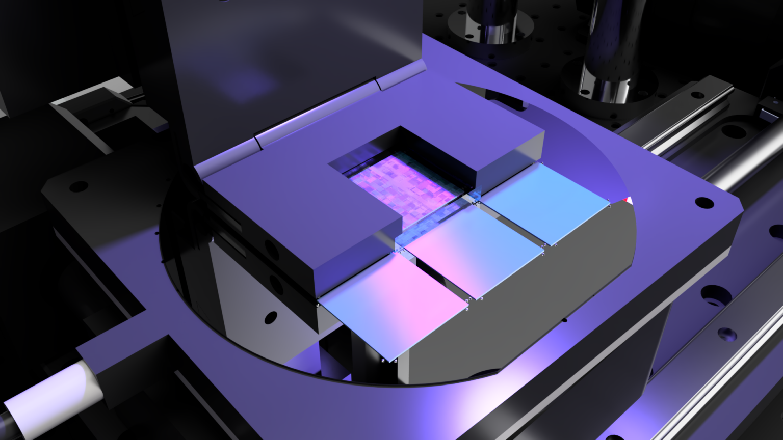
A one-stop Step & Repeat Nanoimprint Lithography Machine
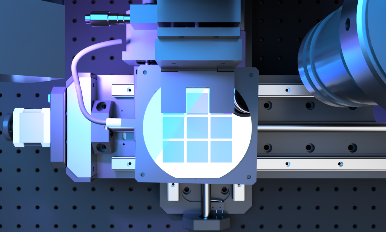
Step & Repeat Nanoimprint Lithography is a highly scalable technique in nanotechnology manufacturing for duplicating intricate patterns onto moulds and minuscule devices.
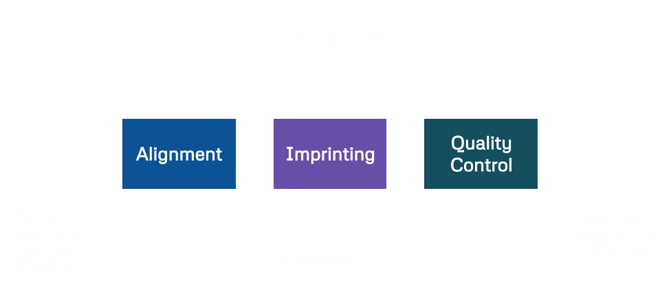
Features and subsystems
Fast, Reliable and Scalable Imprinting
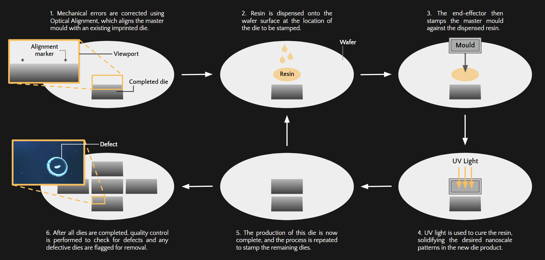
The imprinting subsystem covers every crucial step from dispensing resin to stamping the master mould, creating new moulds. By fully automating such machine performance, the nanoimprint lithography process is sped up by displacing numerous time-consuming, manual practices.
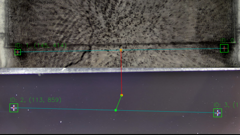
Automatic Alignment using Computer Vision
Computer Vision is utilised to prevent misalignment by automatically correct mechanical errors using the alignment markers (AMs) of each die.
Automated Quality Control and Defect Detection
Our Computer Vision model performs automated defect detection to identify defective dies to be removed. This fast and automated approach reduces cost and manpower requirements.
Previous
Next
The Process
Added value
Inexpensive
200x Lower initial cost: Our compact tabletop design reduces the high expenses associated with EBL, offering an affordable solution while maintaining high-quality results.
Fast and Robust
5x Increase in alignment speed: By displacing manual tasks in the nanoimprinting process with precision machinery, throughput and quality are greatly increased.
Automated
No human intervention required: The use of computer vision and AI for alignment and quality control eliminates the need for human intervention.
At Singapore University of Technology and Design (SUTD), we believe that the power of design roots from the understanding of human experiences and needs, to create for innovation that enhances and transforms the way we live. This is why we develop a multi-disciplinary curriculum delivered v ia a hands-on, collaborative learning pedagogy and environment that concludes in a Capstone project.
The Capstone project is a collaboration between companies and senior-year students. Students of different majors come together to work in teams and contribute their technology and design expertise to solve real-world challenges faced by companies. The Capstone project will culminate with a design showcase, unveiling the innovative solutions from the graduating cohort.
The Capstone Design Showcase is held annually to celebrate the success of our graduating students and their enthralling multi-disciplinary projects they have developed.